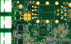
How HDI Printed Circuit Board Design Contributes to Miniaturization
HDI Printed Circuit Board Design
The advancement of portable electronic devices continues to push technology further to produce products that do more and weigh less. This is due to high-performance PCBs that can incorporate a variety of mini-components and thinner materials into a smaller package, without losing quality or speed. One of the leading contributors to this miniaturization is HDI printed circuit board design. The design process for hdi is a complex one that requires specialized equipment, highly skilled technicians, and rigorous quality control procedures to ensure precision in the manufacturing process.
The key to the success of hdi printed circuit board is their higher wiring density, which allows for fewer layers, and reduced size and weight. This is possible due to the use of buried and blind vias, which reduce the space used for interconnections between the layers. This feature also makes them more flexible and versatile than conventional PCBs, allowing them to be placed in smaller spaces in the device and still have adequate functionality.
In addition, HDI PCBs are often cheaper than conventional PCBs in the long run due to their lower cost of raw material. They are also more cost-effective in the short run because they require fewer layers and a smaller board area to function. This makes them an excellent choice for small products and applications that need to be slim and lightweight.
How HDI Printed Circuit Board Design Contributes to Miniaturization
HDI circuit board designs are particularly effective in the medical industry. They can be used in devices like imaging and lab equipment, as well as implants and diagnostic tools. These applications make it essential for these devices to be compact and lightweight, but they must also be able to provide the right level of performance. HDI PCBs are able to achieve this by providing the necessary level of reliability while minimizing their overall weight.
Using the plated microvia technique, it is possible to eliminate some of the layers on the PCB, which can help save on materials and lead times. This is possible through a technique known as via-in-pad (VIP), which involves the formation of a small copper pad on the top of the layer, which is then filled with one of a number of different fill types and capped. The resulting via connects to the internal layer, reducing the amount of metal required on each layer and increasing the overall board density.
Another way to increase the density of an HDI circuit board is to move some of the signal layers to the bottom of the stackup, utilizing the conductive through-hole (CTB) technique. This can be done by moving the GND and PWR layers to the bottom of the stackup, replacing them with microvias, or simply by avoiding them altogether.
In addition, the use of HDI technology in a product can save on space and power by eliminating unnecessary components and reducing the thickness of the circuit board. It can also improve the reliability of the circuit, preventing heat build-up and enhancing signal transmission.